
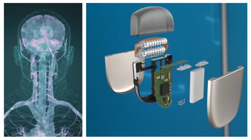
Redefining functionality standards, these reliability-driven substrates offer unrivalled configurable composition for body-friendly PCBs. therefore, these next gen substrates for neuro implants solutions offer a “regular” splendid total thickness 1.2 mm. Meanwhile, sizes can get even smaller with thickness measured by the microns. Some of the systems packaged are already operational and proven in spinal cord implantable stimulation device.
“If a technological feat is possible, man will do it. Almost as if it is wired into the core of our being”. Approximately 37 years after a Cyber punk classic debut, it’s words ring true than ever. Moreover, current tech advancements render what was once fiction as potential reality. In the field of inner-body healthcare, there is no exception. However, the natural conditions of the inner human body demand highly reliable, highly durable and bottom-line hardened treatment solutions. Especially packaged modules designed to withstand the extreme. Nowadays, challenges arise with a new phase in smart implantable devices aimed to ease the lives of patients. Fundamentally reshaping Human Machine Interface (HMI).
To meet the stringent demands of inner-body operations, the solution needs to be biocompatible. In order to meet the demand for biocompatible next gen implanted tech, E.D.E. Electronics is proud to present these body friendly next gen substrates for Neuro implants technology. Designed and made by E.D.E.’s strategic partner Micro Systems Technologies (MST), these substrates are already used in a vast array of inner-body designated solutions such as pacemakers, cardiac monitors, defibrillators and even spinal cord stimulation solutions.
With over 60 years of experience delivering over 300 different solutions for inner-body applications, these next gen substrates for neuro implants tech are field ready and field tested. As volume is a fundamental factor in inner-body implementation, these substrates are offered with a maximum strip thickness “tag” of 1.2 mm. In parallel, the thinnest strip thickness amounts to 150 microns.
From electronic assemblies to full systems solutions, our strategic partner can provide an in-house fabrication process. Thus, offering integration and modulation in a variety of fields. such as battery manufacture, PCBs assembly, semiconductor packaging and much more.
In addition, these substrates and PCBs for body friendly implantable solutions are highly customizable making them the ideal choice for your smart implant configuration. Notwithstanding, these solutions can provide end-to-end traceability. By being able to reduce time to market and optimize costs due to pre-existing fabrication platforms and processes. As all these solutions are FDA approved, MST offers a time to market advantage and reduced costs.
Interestingly, these tech frames are poised to help treatments in epilepsy, abdominal pain and other head related applications. Meanwhile, pre-existing production processes and know-how will enable initial prototype of your idea to be delivered within six months. While further development will produce an end-user friendly convolution within one year.
In continuation, E.D.E. recently introduced a video showcasing MST’s multilayered PCBs configurations designed to endure extreme environments such as space and high endurance aeronautics applications, telecommunications and AI age operations that require highly rugged, highly durable and reliability-driven “tech frames”.